G-OSD mod – new input
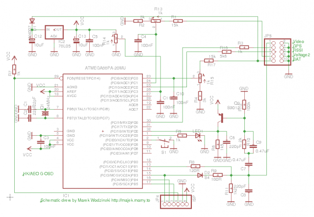
G-OSD schematic diagram and making new analog input to it.
I was very curious how everything is connected in G-OSD. It is similar to E-OSD but different – they added potientiometers, analog inputs and gps. And there was also one mystery: third pot that trims RSSI and do nothing in CL-OSD🙂
So, I made it:
Some conclusions from this schematic arrived:
– third pot really does nothing unless you want to measure 5V from voltage regulator 🙂
– acording to resistor values in voltage dividers, maximum voltage on both inputs could be as high as 23V. I don’t know at how high voltage is rated 10uF capacitor (probably it’s 50V) on battery input, so be carefull with this input. But on Voltage2 it is safe to apply up to 24V.
– video generation circuit is exactly the same as in E-OSD
– pin for RSSI haven’t filtering capacitor, so it could be used also as digital input (for example for measuring RSSI PWM directly from FrSky receiver)
And I used opportunity to make something based on information I learned from schematic and pcb investigation: new analog input! 🙂
So, I made useless pot useful 🙂
Warning: this input has some limitations:
– low input resistance (1kOhm), so it’s not good for current sensor as it require at least 4.7k. Some simple RSSI pwm converters based on passive elements could also work wrong with it.
– voltage from pot goes directly to processor, so putting voltage higher than 5V and turning around this pot without extreme care could end up with death of uC
If you want to measure voltage higher than 5V, put additional resistor in series with this input to be safe. For example for 3C battery, use 2k or 2.2k. If you want more, the rule is: 1kOhm (or more) for every additional 5V.
Now you know limitations of this new input, so let’s do this 🙂
This is my second mod (here is previous), so don’t be surprised by additional pins on pictures, it’s still G-OSD 🙂
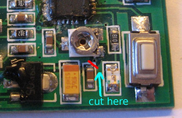
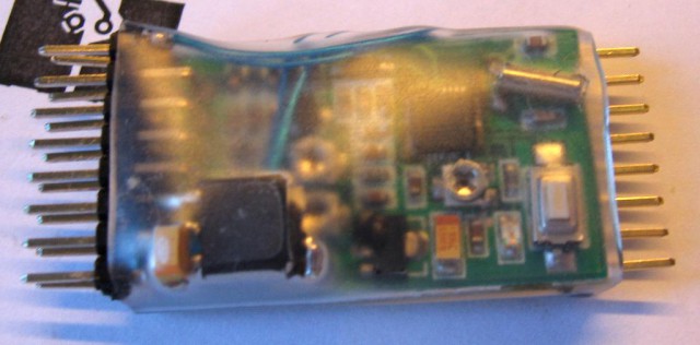
At start (it’s obvious 🙂 ) you should remove shrinkwrap. Then locate third pot (RSSI) and capacitor below it. Please observe that between them there is also a via (small drill/hole). You must cut trace (under white paint) between capacitor and the via as shown on picture:
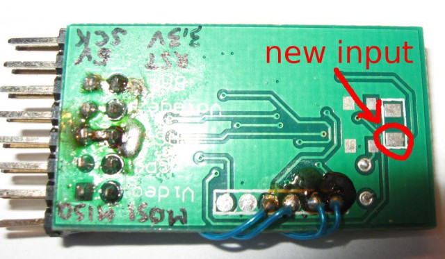
And then you have on opposite side of pcb quite large pad to solder new input:
Do you want it look well and professional? Stay with me for another few pictures 🙂
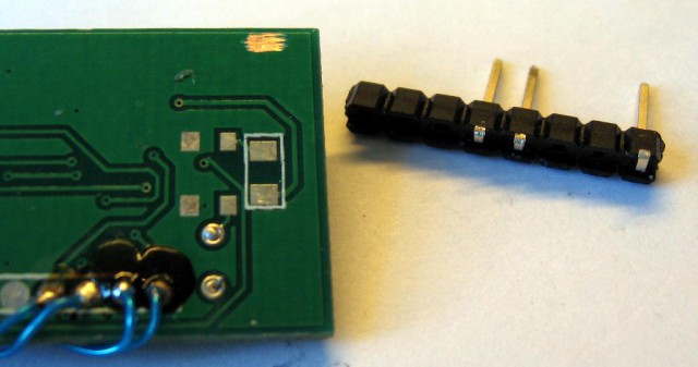
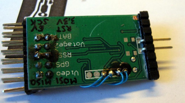
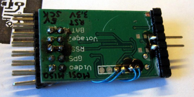
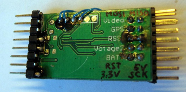
Get new angle pinheader, remove unnecessary pins and cut middle two pins to the edge of plastic as on this picture:
Get CA and glue pinheader to pcb with pins in right position:
After few seconds everything is steady, so you could easily solder pins to pads below:
Now you have one pad connected to new input, second one you can connect by wire to some near gnd pad.
Now you can put new heat wrap, and that’s all.
But…
I don’t like make things twice, so I put few addidtional pins as RFU (and there will be nice to connect i2c and tx pins in future 🙂 )

Hi Majek!
Thanks for your article and schematics!
I figure you have some understanding on how this G-OSD works… Perhaps you could help me with my problem: my video goes BW when I connect my camera to OSD. It does flicker BW/Color but stays BW most of the time…
The camera alone does give a clean color image. Any ideas what I could do?
Thanks for your time,
Dmitry.
Hello Dmitry
Did you checked your connections for ground loop? If you connect ground in wrong way, a weird things happen (up to video signal loss). G-OSD itself shouldn’t influence colour – in fact it makes modifications to video signal only where characters are – other parts of signal is untouched. Try to rewire connections and check if it helps. I had similar problem (poor colour and sometimes synchronization lost) and I solved it by disconnecting redundant ground wires.
If you power video from the same battery as motor, I’m pretty sure you have at least two grounds connected to the osd – one on video side, second from battery and it forms a loop with ground for powering video TX. Leave only one ground connected to OSD and it should help.
Or try to test this with separate battery for video equipment.
Hey Majek!
Thanks for your reply!
I was thinking about thiese ground issues as-well, but the strange thing is that I have a second G-OSDII (bought both at once -> should be the same batch), that works just fine with the same cable!
Ok, but I get your point… I will try to re-solder the elements on the board – perhaps some cold-joint issue…
(By the way, I accidentally broke a Quartz leg – do you know the specs exactly? Apart from it being 24Mhz)
I don’t think that it could be cold-joint. Your signal is weaker, so maybe R11/C8 have bad values. Or there is some short-circuit somewhere.
Do you have proper OSD graphics?
Regarding quartz – any 24MHz should work but I think that there will be hard to buy in such small package – standard HC49 should be no problem.
Hey, perhaps we should switch to email conversation, you should have mine, since it is necessary to enter prior sending this reply…
Today I got the same effect with the second OSD :(.
I got an impression, that new heat-shrink might be the reason for that (well, not the shrink itself, but the process of putting it ;)… Or that it is physically rather close to my VTx…
I think OSD text is clean, it is hard to tell though…
Will check the R11/C8 chain and short circuits…
Thanks again,
Dmitry.
Hello,
I was wondering if you still have the Eagle files for this OSD? I wanted to play around a bit with it but still learning eagle PCB.
I have only schematic: https://majek.sh/modele/g-osd.sch
I hope it helps 🙂
How we can read and show the value for this #3 input?